- 您现在的位置:买卖IC网 > Sheet目录17368 > NCP3011GEVB (ON Semiconductor)BOARD EVAL NCP3011 BUCK CTLR
�� �
�
�NCP3011,� NCV3011�
�V� out� =� 3.3� V�
�18� V�
�12� V�
�I� PP� +�
�LP� CU� +� I� RMS� 2� @� DCR�
�18�
�17�
�16�
�15�
�14�
�13� 15� V�
�12�
�11�
�10�
�9�
�8�
�7�
�6�
�5�
�4�
�3� 9V�
�2�
�1�
�0�
�10%� 15%� 20%� 25%� 30%� 35%� 40%�
�V� IN� ,� (V)�
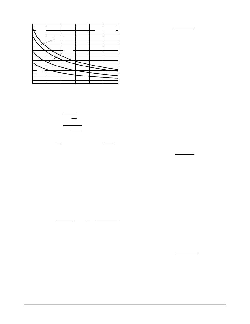
�Figure� 42.� Ripple� Current� Ratio� vs.� Inductance�
�To� keep� within� the� bounds� of� the� parts� maximum� rating,�
�calculate� the� RMS� current� and� peak� current.�
�V� OUT� (1� *� D)�
�(eq.� 14)�
�L� OUT� @� F� SW�
�Ipp� is� the� peak� to� peak� current� of� the� inductor.� From� this�
�equation� it� is� clear� that� the� ripple� current� increases� as� L� OUT�
�decreases,� emphasizing� the� trade� ?� off� between� dynamic�
�response� and� ripple� current.�
�The� power� dissipation� of� an� inductor� consists� of� both�
�copper� and� core� losses.� The� copper� losses� can� be� further�
�categorized� into� dc� losses� and� ac� losses.� A� good� first� order�
�approximation� of� the� inductor� losses� can� be� made� using� the�
�DC� resistance� as� they� usually� contribute� to� 90%� of� the� losses�
�of� the� inductor� shown� below:�
�(eq.� 15)�
�The� core� losses� and� ac� copper� losses� will� depend� on� the�
�geometry� of� the� selected� core,� core� material,� and� wire� used.�
�Most� vendors� will� provide� the� appropriate� information� to�
�make� accurate� calculations� of� the� power� dissipation� then� the�
�1� )� ra� 3� 8.02� A�
�I� RMS� +� I� OUT� @�
�2�
�12�
�(eq.� 11)�
�total� inductor� losses� can� be� capture� buy� the� equation� below:�
�LP� tot� +� LP� CU_DC� )� LP� CU_AC� )� LP� Core� (eq.� 16)�
�+� 8A� @�
�1� )�
�(0.23)� 2�
�12�
�Input� Capacitor� Selection�
�The� input� capacitor� has� to� sustain� the� ripple� current�
�I� PK� +� I� OUT� @� 1� )�
�ra�
�2�
�3� 8.92� A� +� 8� A� @� 1� )�
�(0.23)�
�2�
�(eq.� 12)�
�produced� during� the� on� time� of� the� upper� MOSFET,� so� it�
�must� have� a� low� ESR� to� minimize� the� losses.� The� RMS� value�
�of� this� ripple� is:�
�SlewRate� LOUT� +� 3� 2.6� +�
�L� OUT�
�(eq.� 18)�
�I� INRUSH� +�
�An� inductor� for� this� example� would� be� around� 3.3� m� H� and�
�should� support� an� rms� current� of� 8.02� A� and� a� peak� current�
�of� 8.92� A.�
�The� final� selection� of� an� output� inductor� has� both�
�mechanical� and� electrical� considerations.� From� a�
�mechanical� perspective,� smaller� inductor� values� generally�
�correspond� to� smaller� physical� size.� Since� the� inductor� is�
�often� one� of� the� largest� components� in� the� regulation� system,�
�a� minimum� inductor� value� is� particularly� important� in�
�space� ?� constrained� applications.� From� an� electrical�
�perspective,� the� maximum� current� slew� rate� through� the�
�output� inductor� for� a� buck� regulator� is� given� by� Equation� 13.�
�V� IN� *� V� OUT� A 12 V� *� 3.3 V�
�m� s� 3.3� m� H�
�(eq.� 13)�
�This� equation� implies� that� larger� inductor� values� limit� the�
�regulator� ’s� ability� to� slew� current� through� the� output�
�inductor� in� response� to� output� load� transients.� Consequently,�
�output� capacitors� must� supply� the� load� current� until� the�
�inductor� current� reaches� the� output� load� current� level.� This�
�results� in� larger� values� of� output� capacitance� to� maintain�
�tight� output� voltage� regulation.� In� contrast,� smaller� values� of�
�inductance� increase� the� regulator� ’s� maximum� achievable�
�slew� rate� and� decrease� the� necessary� capacitance,� at� the�
�expense� of� higher� ripple� current.� The� peak� ?� to� ?� peak� ripple�
�current� for� the� NCP3011� is� given� by� the� following� equation:�
�Iin� RMS� +� I� OUT� @� D� @� (1� *� D)� (eq.� 17)�
�D� is� the� duty� cycle,� Iin� RMS� is� the� input� RMS� current,� and�
�I� OUT� is� the� load� current.�
�The� equation� reaches� its� maximum� value� with� D� =� 0.5.�
�Loss� in� the� input� capacitors� can� be� calculated� with� the�
�following� equation:�
�2�
�P� CIN� +� ESR� CIN� @� I� IN� *� RMS�
�P� CIN� is� the� power� loss� in� the� input� capacitors� and� ESR� CIN�
�is� the� effective� series� resistance� of� the� input� capacitance.�
�Due� to� large� dI/dt� through� the� input� capacitors,� electrolytic�
�or� ceramics� should� be� used.� If� a� tantalum� must� be� used,� it�
�must� by� surge� protected.� Otherwise,� capacitor� failure� could�
�occur.�
�Input� Start� ?� up� Current�
�To� calculate� the� input� startup� current,� the� following�
�equation� can� be� used.�
�C� OUT� @� V� OUT�
�(eq.� 19)�
�t� SS�
�I� inrush� is� the� input� current� during� startup,� C� OUT� is� the� total�
�output� capacitance,� V� OUT� is� the� desired� output� voltage,� and�
�t� SS� is� the� soft� start� interval.� If� the� inrush� current� is� higher� than�
�the� steady� state� input� current� during� max� load,� then� the� input�
�fuse� should� be� rated� accordingly,� if� one� is� used.�
�http://onsemi.com�
�22�
�发布紧急采购,3分钟左右您将得到回复。
相关PDF资料
MIC2505BM
IC SW HIGH SIDE SGL 2A 8SOIC
MIC2505-2BM
IC SW HIGH SIDE SGL 2A 8SOIC
MIC2505-1BM
IC SW HIGH SIDE SGL 2A 8SOIC
TAAB106K020G
CAP TANT 10UF 20V 10% AXIAL
MC34063LBBEVB
EVAL BOARD FOR MC34063LBB
A9BAG-0502F
FLEX CABLE - AFF05G/AF05/AFE05T
EBM08DTMD-S189
CONN EDGECARD 16POS R/A .156 SLD
RCM06DSUI
CONN EDGECARD 12POS DIP .156 SLD
相关代理商/技术参数
NCP3012
制造商:ONSEMI 制造商全称:ON Semiconductor 功能描述:Synchronous PWM Controller
NCP3012DTBR2G
功能描述:电压模式 PWM 控制器 Single Output Buck 0.8V to 40V 70uA RoHS:否 制造商:Texas Instruments 输出端数量:1 拓扑结构:Buck 输出电压:34 V 输出电流: 开关频率: 工作电源电压:4.5 V to 5.5 V 电源电流:600 uA 最大工作温度:+ 125 C 最小工作温度:- 40 C 封装 / 箱体:WSON-8 封装:Reel
NCP301HSN09T1
功能描述:电压监测器/监控器 0.9V Detector RoHS:否 制造商:Texas Instruments 监测电压数:2 监测电压:Adjustable 输出类型:Open Drain 欠电压阈值: 过电压阈值: 准确性:1 % 工作电源电压:1.5 V to 6.5 V 工作电源电流:1.8 uA 最大工作温度:+ 125 C 封装 / 箱体:SON-6 安装风格:SMD/SMT
NCP301HSN09T1G
功能描述:电压监测器/监控器 0.9V Detector w/Reset High RoHS:否 制造商:Texas Instruments 监测电压数:2 监测电压:Adjustable 输出类型:Open Drain 欠电压阈值: 过电压阈值: 准确性:1 % 工作电源电压:1.5 V to 6.5 V 工作电源电流:1.8 uA 最大工作温度:+ 125 C 封装 / 箱体:SON-6 安装风格:SMD/SMT
NCP301HSN10T1
制造商:ONSEMI 制造商全称:ON Semiconductor 功能描述:Voltage Detector Series
NCP301HSN11T1
制造商:ONSEMI 制造商全称:ON Semiconductor 功能描述:Voltage Detector Series
NCP301HSN12T1
制造商:ONSEMI 制造商全称:ON Semiconductor 功能描述:Voltage Detector Series
NCP301HSN13T1
制造商:ONSEMI 制造商全称:ON Semiconductor 功能描述:Voltage Detector Series